How the EU-Funded POWERBASE Project is Revolutionizing Power Electronics: A 2026 Guide for UK Manufacturers Exploring Gallium Nitride and Silicon Carbide Innovations
How the EU-Funded POWERBASE Project is Revolutionizing Power Electronics: A 2026 Guide for UK Manufacturers Exploring Gallium Nitride and Silicon Carbide Innovations
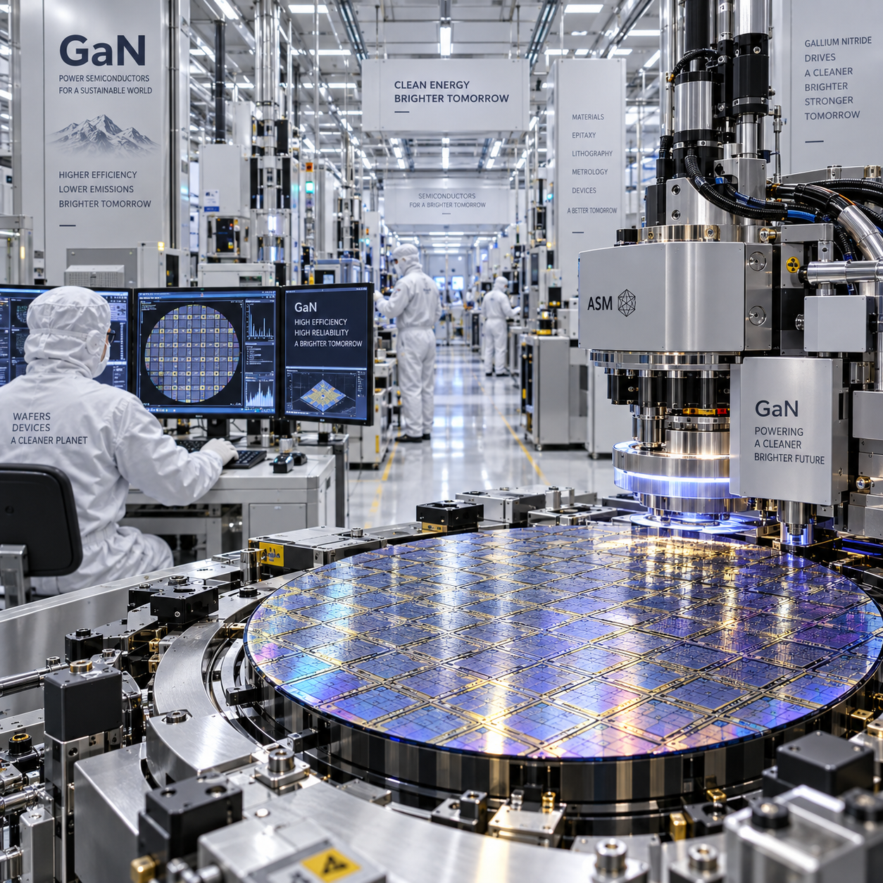
I've spent a fair bit of time this year talking to engineering teams across the UK who are trying to figure out whether gallium nitride and silicon carbide are worth the investment, or whether they're just industry buzzwords dressed up in marketing slides. The honest answer is that these materials are genuinely changing how power electronics gets built, and one of the biggest reasons why is a European research initiative called POWERBASE. If you're running a manufacturing operation in the UK and haven't looked closely at this project, now's a good time to start paying attention.
What Is the POWERBASE Project and Why It Matters in 2026
POWERBASE is an EU-funded collaborative research programme focused on pushing gallium nitride (GaN) and silicon carbide (SiC) power electronics from lab curiosities into mainstream, cost-effective manufacturing. It brings together semiconductor fabs, research institutes, and industrial partners across Europe to solve the practical problems that have historically kept these wide-bandgap materials expensive and difficult to scale.
Now, you might be wondering why a UK manufacturer should care about an EU initiative post-Brexit. Fair question. But supply chains for power semiconductors don't respect political borders. The equipment, wafer suppliers, and technical standards that come out of projects like this one ripple through the entire European industrial ecosystem, UK included. If your company sources components or collaborates with continental partners—which most power electronics firms still do—the innovations coming out of POWERBASE will eventually land on your production floor whether you engaged directly or not.
The Origins and Goals of the Initiative
The project launched with a clear mandate: reduce the cost and complexity of manufacturing GaN and SiC power devices while improving their reliability for demanding applications. The consortium includes chip fabricators, automotive suppliers, and academic research centres, all working toward shared goals around wafer processing, packaging innovations, and device integration. It's not a single company's pet project—it's a genuinely collaborative effort with real industrial stakes attached.
Gallium Nitride vs Silicon Carbide: Key Differences UK Manufacturers Should Know
I get asked constantly which material is 'better,' and the truthful response is that it depends entirely on your application. GaN tends to shine in high-frequency switching applications where compact size and speed matter most, think power adapters, RF amplifiers, and increasingly, EV onboard chargers. SiC, on the other hand, handles higher voltage and thermal loads more gracefully, making it the go-to choice for traction inverters, industrial motor drives, and renewable energy inverters where ruggedness under sustained load is non-negotiable.
Cost is still a factor worth weighing carefully. SiC wafers remain pricier per unit area than silicon, though prices have dropped noticeably over the past couple of years as manufacturing volumes increase. GaN devices, meanwhile, have become remarkably affordable for lower-power applications but still face scaling challenges at higher voltage tiers.
Performance Benchmarks in Real-World Applications
On UK production lines I've seen testing, GaN devices routinely achieve switching frequencies several times higher than traditional silicon MOSFETs, translating directly into smaller magnetics and lighter overall system weight. SiC devices, by comparison, demonstrate superior thermal conductivity and can operate reliably at junction temperatures exceeding 150°C without the same derating penalties silicon-based parts suffer. For manufacturers building compact power supplies or EV charging infrastructure, these aren't marginal improvements—they're the difference between a competitive product and an obsolete one.
How POWERBASE Is Advancing Manufacturing Processes
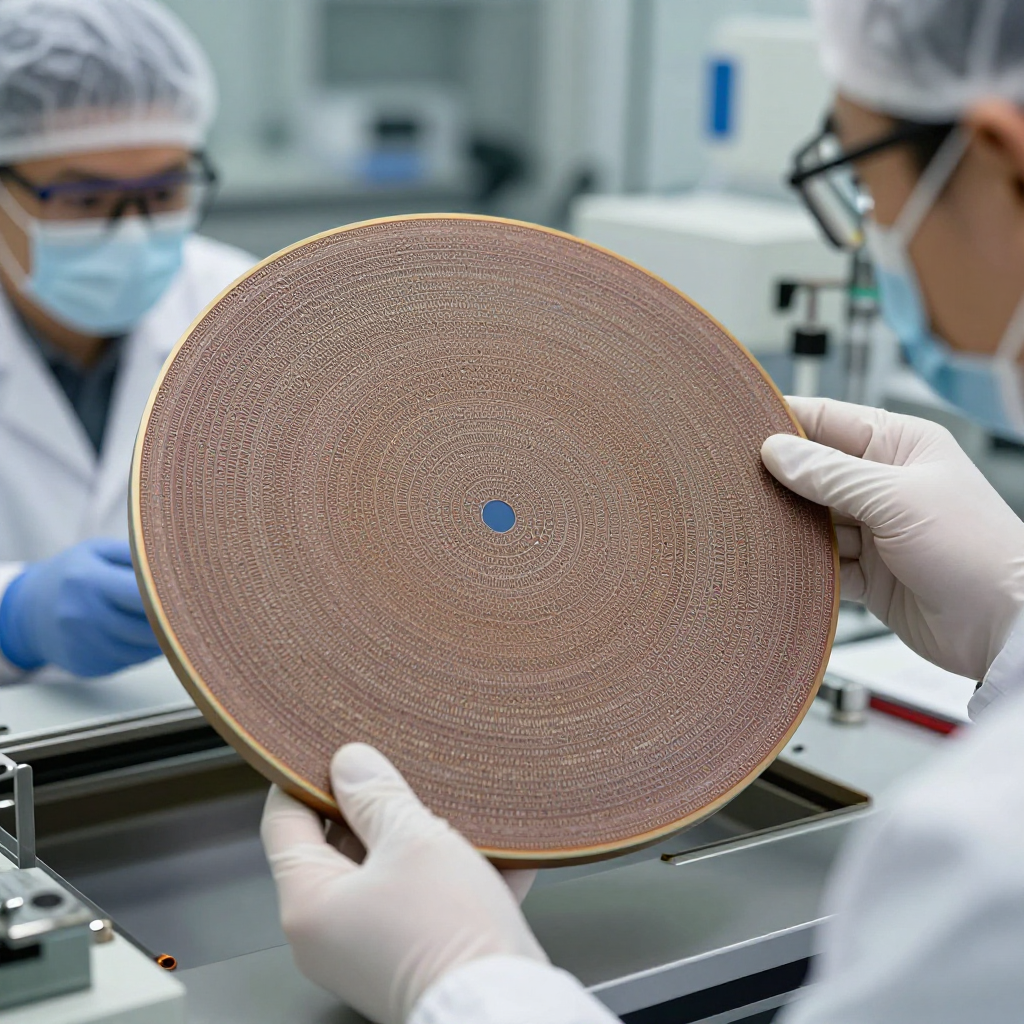
What makes POWERBASE particularly relevant to manufacturers rather than just academics is its focus on wafer-level integration techniques and fabrication process improvements that directly reduce production costs. The project has contributed advances in epitaxial growth quality, device packaging that reduces parasitic inductance, and testing methodologies that catch defects earlier in the production cycle—all of which translate into fewer scrapped wafers and better yield rates.
If you want to dig into the technical documentation, published outcomes, and ongoing research updates, the project maintains detailed resources at https://powerbase-project.eu/. I'd recommend bookmarking it if your R&D team is evaluating GaN or SiC integration into new product lines, since the published papers and process guidelines offer a genuinely useful shortcut past a lot of trial-and-error that smaller manufacturers simply can't afford.
Benefits for UK Manufacturers Adopting These Technologies
The practical upside here is substantial. Switching to GaN or SiC components typically means smaller heat sinks, reduced passive component counts, and meaningfully improved energy efficiency—often in the range of several percentage points, which sounds modest until you multiply it across thousands of units shipped annually. For manufacturers targeting EV charging infrastructure or renewable energy inverters, that efficiency gain directly improves product competitiveness in a crowded international market.
There's also a compliance angle worth mentioning. As UK regulations increasingly push toward stricter energy efficiency standards for industrial and consumer electronics, having wide-bandgap semiconductor expertise in-house positions manufacturers well ahead of tightening requirements rather than scrambling to catch up later.
Aligning with UK Net-Zero and Industrial Strategy
The UK government's net-zero commitments create real pressure—and real opportunity—for manufacturers who move early on power electronics efficiency. GaN and SiC adoption directly supports decarbonization goals by reducing energy losses across everything from data centre power supplies to EV drivetrains. It also strengthens domestic manufacturing resilience, an increasingly important consideration as post-Brexit supply chain vulnerabilities have made UK industry rethink its dependence on distant, single-source suppliers.
Common Challenges and Mistakes to Avoid During Adoption
I've watched a few UK manufacturers stumble in predictable ways when adopting these materials, so it's worth flagging the usual suspects:
- Underestimating thermal management requirements—GaN and SiC devices switch faster and run hotter in localized areas than engineers expect, and inadequate cooling design leads to premature failures.
- Sourcing from unreliable or inconsistent wafer suppliers, which can introduce variability that wrecks production yield and reliability testing.
- Ignoring the skills gap—there simply aren't enough UK engineers with deep wide-bandgap semiconductor experience yet, and treating this as a plug-and-play swap for silicon components almost always backfires.
None of these are dealbreakers, but they do require honest planning rather than optimistic assumptions borrowed from silicon-era design practices.
Practical Steps for UK Manufacturers to Get Started
If you're serious about moving into GaN or SiC manufacturing, start by building relationships with UK research institutions and universities that already have wide-bandgap semiconductor labs—several are actively collaborating with European partners on related work. Look into available funding streams through Innovate UK and sector-specific grants aimed at power electronics innovation. Invest early in upskilling your engineering team, whether through targeted training programmes or hiring specialists with direct GaN/SiC design experience. And frankly, keep an eye on ongoing POWERBASE publications and technical updates, since emerging best practices and standards coming out of that consortium will likely shape industry expectations well before UK-specific standards catch up.
Frequently Asked Questions
Is POWERBASE still relevant for UK collaboration post-Brexit? Yes. While formal EU funding mechanisms differ for UK entities now, the technical outputs, published research, and industry standards emerging from the project remain openly accessible and highly relevant to UK manufacturers working within shared European supply chains.
Which industries benefit most from this technology shift? Automotive (particularly EV charging and traction systems), renewable energy inverters, industrial power supplies, and data centre power management are seeing the most immediate gains.
How does GaN/SiC adoption affect manufacturing costs in 2026? Initial tooling and material costs remain higher than traditional silicon, but falling wafer prices combined with efficiency gains and reduced component counts are steadily narrowing the total cost of ownership gap, particularly for high-volume applications.